- 您现在的位置:买卖IC网 > Sheet目录39246 > LM2685MTCX/NOPB (NATIONAL SEMICONDUCTOR CORP) SWITCHED CAPACITOR REGULATOR, 180 kHz SWITCHING FREQ-MAX, PDSO14
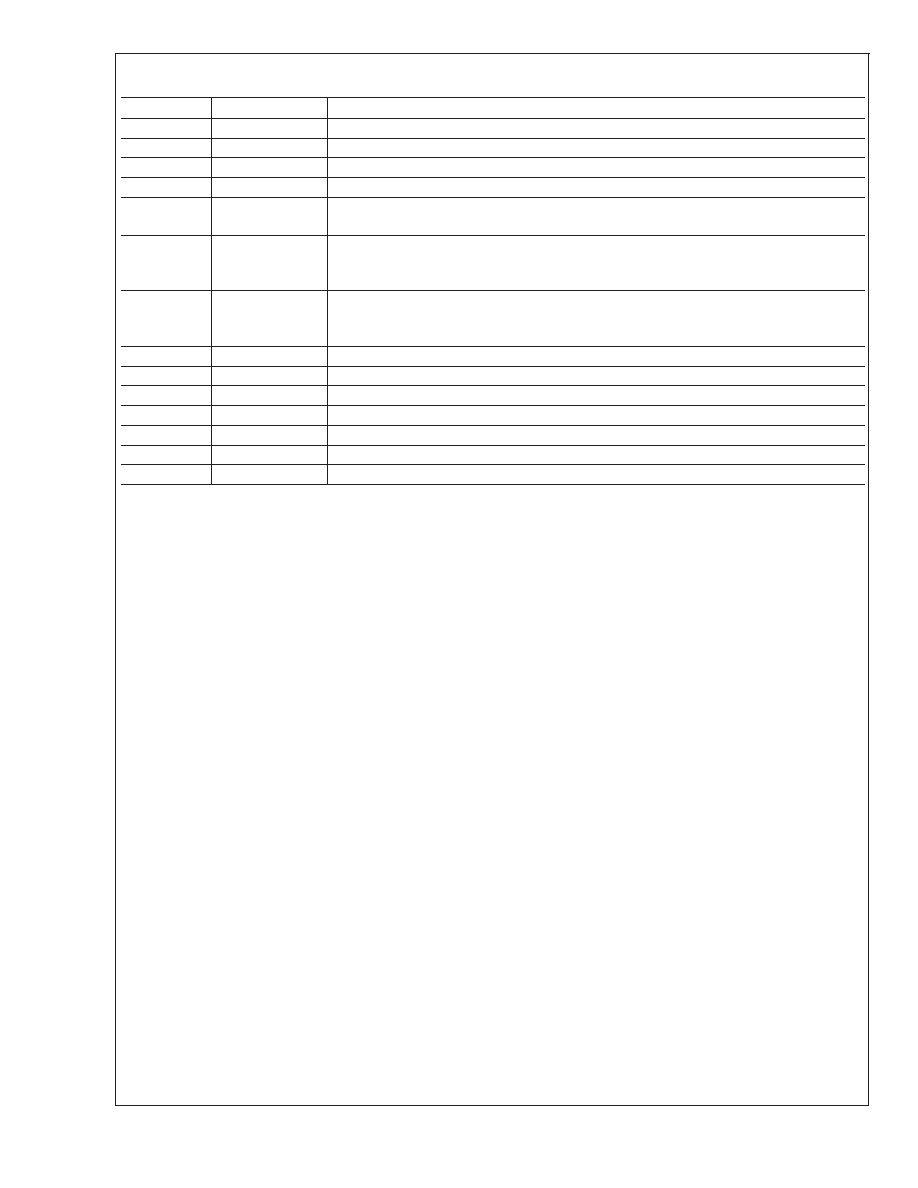
Pin Description
Pin No.
Name
Function
1V
IN
Power supply input voltage.
2
GND
Power supply ground.
3V
NEG
Negative output voltage created by inverting V
05.
4V
NSW
V
NEG output connected through a series switch, NSW.
5
CE
Chip enable input. This pin is high for normal operation and low for shutdown. (See
Shutdown and Load Disconnect section in the Detailed Device Description division).
6
SDP
Positive side shutdown input. This pin is low for normal operation and high for positive
side shutdown and V
PSW load disconnect. (See Shutdown and Load Disconnect section in
the Detailed Device Description division).
7
SDN
Negative side shutdown input. This pin is low for normal operation and high for negative
side shutdown and V
NSW load disconnect. (See Shutdown and Load Disconnect section in
the Detailed Device Description division).
8C
2
The negative terminal of inverting charge-pump capacitor, C2.
9C
2
+
The positive terminal of inverting charge-pump capacitor, C2.
10
V
05
Regulated +5V output.
11
V
PSW
V
05 output connected through a series switch, PSW.
12
V
DBL
Voltage Doubler Output. (2.85V
≤ V
IN
≤ 5.4V. See Voltage Doubler section).
13
C
1
+
The positive terminal of doubling charge-pump capacitor, C1.
14
C
1
The negative terminal of doubling charge-pump capacitor, C1.
LM2685
www.national.com
2
发布紧急采购,3分钟左右您将得到回复。
相关PDF资料
LM2686MTCX/NOPB
SWITCHED CAPACITOR REGULATOR, 180 kHz SWITCHING FREQ-MAX, PDSO14
LM2787BPX/NOPB
0.01 A SWITCHED CAPACITOR REGULATOR, 450 kHz SWITCHING FREQ-MAX, PBGA8
LM2787TP/NOPB
0.01 A SWITCHED CAPACITOR REGULATOR, 450 kHz SWITCHING FREQ-MAX, PBGA8
LM2787BP/NOPB
0.01 A SWITCHED CAPACITOR REGULATOR, 450 kHz SWITCHING FREQ-MAX, PBGA8
LM285AH-1.2
1-OUTPUT TWO TERM VOLTAGE REFERENCE, 1.235 V, MBCY2
LM185AYH-1.2
1-OUTPUT TWO TERM VOLTAGE REFERENCE, 1.235 V, MBCY2
LM185AH-1.2
1-OUTPUT TWO TERM VOLTAGE REFERENCE, 1.235 V, MBCY2
LM285BEOA-2.5713
1-OUTPUT TWO TERM VOLTAGE REFERENCE, 2.5 V, PDSO8
相关代理商/技术参数
LM2686MTC
制造商:Texas Instruments 功能描述:VOLT CONVERTER SMD 2686 TSSOP14
LM2686MTC
制造商:Texas Instruments 功能描述:VOLT CONVERTER SMD 2686 TSSOP14
LM2686MTC/NOPB
功能描述:IC REG SWITCHED CAP DBL 14-TSSOP RoHS:是 类别:集成电路 (IC) >> PMIC - 稳压器 - DC DC 开关稳压器 系列:- 产品培训模块:Lead (SnPb) Finish for COTS
Obsolescence Mitigation Program 标准包装:1 系列:- 类型:降压(降压) 输出类型:固定 输出数:1 输出电压:3.3V 输入电压:4.5 V ~ 24 V PWM 型:- 频率 - 开关:- 电流 - 输出:125mA 同步整流器:无 工作温度:-40°C ~ 85°C 安装类型:表面贴装 封装/外壳:SOT-23-6 包装:Digi-Reel® 供应商设备封装:SOT-6 其它名称:MAX1836EUT33#TG16DKR
LM2686MTCX/NOPB
功能描述:IC REG SWITCHED CAP DBL 14-TSSOP RoHS:是 类别:集成电路 (IC) >> PMIC - 稳压器 - DC DC 开关稳压器 系列:- 产品培训模块:Lead (SnPb) Finish for COTS
Obsolescence Mitigation Program 标准包装:1 系列:- 类型:降压(降压) 输出类型:固定 输出数:1 输出电压:3.3V 输入电压:4.5 V ~ 24 V PWM 型:- 频率 - 开关:- 电流 - 输出:125mA 同步整流器:无 工作温度:-40°C ~ 85°C 安装类型:表面贴装 封装/外壳:SOT-23-6 包装:Digi-Reel® 供应商设备封装:SOT-6 其它名称:MAX1836EUT33#TG16DKR
LM2687LD
制造商:Texas Instruments 功能描述:
LM2687LD/NOPB
功能描述:IC REG SWITCHD CAP INV ADJ 8-LLP RoHS:是 类别:集成电路 (IC) >> PMIC - 稳压器 - DC DC 开关稳压器 系列:- 产品培训模块:Lead (SnPb) Finish for COTS
Obsolescence Mitigation Program 标准包装:1 系列:- 类型:降压(降压) 输出类型:固定 输出数:1 输出电压:3.3V 输入电压:4.5 V ~ 24 V PWM 型:- 频率 - 开关:- 电流 - 输出:125mA 同步整流器:无 工作温度:-40°C ~ 85°C 安装类型:表面贴装 封装/外壳:SOT-23-6 包装:Digi-Reel® 供应商设备封装:SOT-6 其它名称:MAX1836EUT33#TG16DKR
LM2687LDX
功能描述:电荷泵 RoHS:否 制造商:Maxim Integrated 功能:Inverting, Step Up 输出电压:- 1.5 V to - 5.5 V, 3 V to 11 V 输出电流:100 mA 电源电流:1 mA 最大工作温度:+ 70 C 封装 / 箱体:SOIC-8 Narrow 封装:Tube
LM2687LDX/NOPB
功能描述:电荷泵 RoHS:否 制造商:Maxim Integrated 功能:Inverting, Step Up 输出电压:- 1.5 V to - 5.5 V, 3 V to 11 V 输出电流:100 mA 电源电流:1 mA 最大工作温度:+ 70 C 封装 / 箱体:SOIC-8 Narrow 封装:Tube